Focused ion beam scanning electron microscope
SCIOS 2
Acquired 2018
Prerequisite
Proficiency in SEM, i.e. having passed the conventional SEM training and an additional 10-20 hours experience operating the SEM without help or equivalent from past experience.
How-tos and procedures
-
Loading a sample
Preamble
- Load the highest samples on the right side (when standing in front of the microscope) of the stage. In any case, do not load samples that differ strongly in height.
- Keep the stage clean. Use basic household cleaning products.
- Use long stub pins. Short stub pins will not work well.
- Avoid using C-tape to mount samples on a stub. It “sets” over time and may cause therefore drift during ablation. Use colloidal silver instead.
Pumping the stage
- After you mounted the sample, close the chamber door.
- Do not take a NavCam image during pumping. It may be imprecise because o-ring movements during pumping. Better to wait until pumping is finished.
- In the sample exchange window, click Pump.
- Hold your hand / lean against the door until the TMP1 in the vacuum tab of the Sample exchange window shows at least 5%.
Homing the stage while pumping
- Then in the UI: chose Stage > home stage
- This procedure takes less than 1 minute
- Then: move on to the next step: eucentric height
-
Eucentric height
Preamble
Eucentric height is a crucial alignment which must be done with the utmost precision.
Assumptions
- Good vacuum: Chamber pressure 10-2 Pa or better.
- Stage homed
Procedure
- Start the electron beam. Electron column settings:
Magnification < 100X HV 5 kV Beam current 0.1 – 0.8 nA Scan speed 1 us - Start the electron beam and run auto contrast brightness (F9).
- Focus the image.
- Link the stage.
- Lower the Z value of the stage e.g. from 60 mm to 30 mm. Meanwhile, zoom in to 500X. Focus again and link again.
- Again lower the Z stage to e.g. 15 mm. Meanwhile, zoom in to 1000X. Focus and link.
- Lower the Z stage to 7 mm and zoom in to 1000X. Focus and link. Repeat at 7 mm and 5 000X if needed.
- Press CTRL+F
You should now have the stage at exactly 7 mm Z height and perfectly in focus at a magnification of 10 000X
WARNING
Assure you do this alignment on THE HIGHEST POINT OF ALL SAMPLES on the stage!!!
-
Set the beam coincidence point
Preamble
- The eucentric height is set perfectly at 7 mm.
- Reset the beam shifts (beam shift > right click > reset)
Procedure
- Locate a landmark and place it in the middle of the electron beam image. Use a crosshair if needed (View > center cross).
Magnification 5000-10 000 X HV 5 kV Beam current 0.1 – 0.8 nA Scan speed 1 us - Tilt to 5°, use stage Z (in the tab navigation) to move the landmark back to the middle/crosshair. Alternatively: in the camera port, hold the middle mouse button (the cursor becomes a yellow line) and move the mouse down to move the landmark .
- Go in steps (10°, 20°, 40°) to 52°. At 52° the same object (landmark) should be exactly at the cross again. Check with the position with CTRL+e / CTRL+i.
Note: the object might move left/right. That is not relevant.
Note: you will need to do the auto brightness-contrast after tilting.
-
Beam shift the ion and e-beam image
Select a landmark in the SEM image. Place it in the middle of the image
Magnification > 1000 X HV 5 kV Beam current 0.1 – 0.8 nA Scan speed 1 us - Switch on the ion beam. Wait 10 seconds
- run the auto brightness contrast
- Make 1 image with low beam settings (F6 then immediately F6 again)
Magnification 800-1000 X HV 30 kV Beam current 10 pA Scan speed 1 us - Locate the landmark in the ion beam image. Zoom out if needed.
- In the ion beam image: press and hold shift, left click and hold on the landmark. The mouse changes into a hand with blue sleeves. Drag the mouse to the center of the ion beam image (where the crosshair is). Release the mouse and the shift key.
-
Pt deposition of porous structures
Preamble
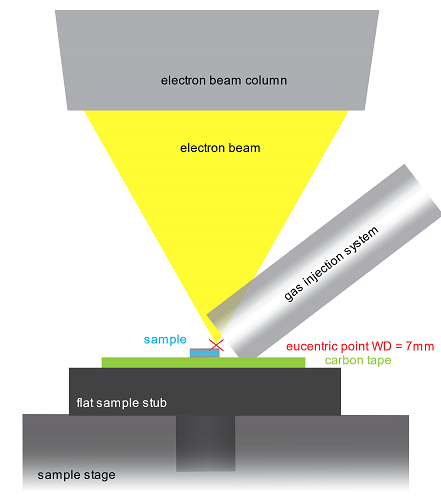
Porous materials, 3D photonic networks, two phase self-assembled structures and similar samples need to be (back)filled to be appropriate for FIBSEM tomography. If not, any subsequent binarization and segmentation (in e.g Avizo) will be biased, if possible. Kenza Djeghdi developed an in-situ platinum filling technique for photonic networks, which yields good contrast and conductivity throughout the analyzed volume.
Important note
The Pt filling process involves high intensity electron beam irradiation for more than 10 minutes (usually 12-20 minutes), hence non-negligible artefacts and deformations may occur in your sample. Compression or shrinking may be expected processes going on during the filling procedure. Please evaluate your results carefully keeping this in mind.
Liability note
Consider your abilities on the instrument. No-one shall be made liable when you follow these instructions. Always evaluate for yourself and consider if the next step is possible in your situation. Do not risk anything that can damage the instrument. Please do not follow these instructions blindly.
Procedure
Requirements
Your sample needs to be porous from the top, in order for the Pt gas precursor to diffuse into the structure before being decomposed by the e-beam irradiation.
- For beetle scales, where the photonic network is wrapped in a cortex, the samples are opened a priori by plasma etching.
- For metamaterials (based on e.g. coblock polymers) one of the phases has to be etched away.
In any case, a continuous air (or void) network has to be present, individual holes in a material (e.g. holes in cheese) cannot be filled this way.
Eucentric height
- Set eucentric height (WD=7 mm + CTRL+f)
- Stage tilt = 0° and absolute sample tilt 0° (if your sample is flat)
Optimize SEM imaging settings
- Change the SEM imaging settings to 30kV, and a high beam current that works for your sample (e.g. 1.6 nA).
- Refocus and correct the astigmatism.
Setup Pt EBID
- Draw a rectangle for deposition (Pt-EBID, green) in the desired spot in the SEM image.
- Set the depth to 1-3µm depending on how deep you want to fill your sample. Note, this depth value is virtual and depends on your sample geometry.
- Update the electron beam current to achieve acceptable deposition times (10-20 minutes)
- The duration of the Pt deposition will generally be longer than for a flat bulk deposition, especially if Z was increased. E.g. for 5x5x4µm this takes about 15min.
Insert the GIS needle and start the patterning
- Insert the GIS and double-check the position of your deposition region
- Start the patterning
Cleanup
- After deposition is finished, retract the GIS needle
- Check the result in SEM imaging, e.g. 5kV, 0.2nA (or your usual imaging parameters).
Credits
Kenza Djeghdi and Viola Bauernfeind.
-
Ion Beam induced platinum deposition
Preamble
The following alignments were properly done:
- Eucentric height
- Perfect beam coincidence point
- Beam shift ion and electron beam
Procedure
- Pt deposition with the Ga ion beam (in the Ga ion image)
- Don’t make an image with the Ga ion beam!
- draw a rectangle in the Ga ion image with the patterning tool (e.g. 20µm x 2µm)
- z= about 1 µm
- Dwell time: 200 ns
- Select Pt dep (not Si) in the application
- Calculate the Ga current required using the magic number 6 (pA/µm2).
- 20 µm x 2µm x 6 = 240 pA
- use this value and chose the closest current for the Ga beam
- This is important! too much current and you will mill instead of deposit
- Too less current you you will destroy your vacuum
- You should get a time round 3-5 minutes
- Insert the Pt GIS
- Press F9 in the ion image (this will contrast/brightness correct and take a snapshot). Make sure you have the ETD selected
- Check the position of the rectangle, overlay the e-beam deposited marker.
- Run the deposition
- retract the GIS needle
-
Cross sections
Preamble
The following alignments were properly done:
- Eucentric height
- Perfect beam coincidence point
- Beam shift ion and electron beam
- Pt deposition
Additional reading
Bulk milling
- Use the regular cross section pattern. Position it just below the Pt deposition you just made with the Ga
- Place the RCS pattern a bit wider than the Pt deposition marker (about 10-20%) and not exactly touching the Pt above it
- Application: Si multipass
- determine / decide on the depth (e.g. 5 µm)
- calculate the Y, with Y> 2 times Z
- Pick a Ga ion beam current to mill between 2-5 minutes (rule of thumb, no calculation needed)
- iSPI is possible. Use the brightnes contrast buttons on the physical control panel to adjust B/C, not F9
Polishing
- Set a tilt angle to correct for the beam shape: somewhere back 0.5-1.5° (i.e. between 50.5° and 51.5° absolute angle)
- Refresh the ion beam image (F9)
- Place a cleaning cross section between the Pt deposition and the edge (or a little bit over it) of the hole the step before made. place is just a little bit into to Pt (is this correct?). Width of the section: about as wide as the Pt deposition
- Go two steps back in beam current (in the list)
- Depth (currently, we think this is Z): 1/4 of the previous setting. If it was 1000 nm in the regular CS, set it to 250 nm now.
- You can use the iSPY: this will stop the patterning temporarily, make a SEM image and continue
Imaging
- Go to a very low ion beam current (10 pA)
- Press F9
- Curtaining issues: Do not use the ETD, since curtaining is the strongest in that detector. Switch to OptiTilt and use T1 and T2.
- Lower beam currents: more focused Beam, but more curtaining.
- To image the object with the FIB:
- Go to 0° tilt
- rotate the stage 180°
- scan rotate 180° (use SHIFT F12)
-
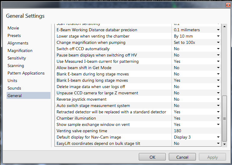
Switch on the light in the chamber
Back light in the FIB can be very helpful when loading the samples. If it is not switched on by default:
- Menu: Tools > Preferences
- In preferences: Entry General (last one)
- Scroll to the bottom of the list, entry Microscope operation
- Find the option: Chamber illumination
- Set it to yes
- Click OK
Brand
ThermoFischer Scios 2 | acquired 2018
Electron optics
- Non-immersion column
- High-stability Schottky field emission gun at 20 eV-30 keV
- 0.9 nm resolution at 30 keV STEM, 1.2 nm at 1 keV with beam deceleration
Ion optics
- Sidewinder ion column with acceleration voltage: 500 V – 30 kV
- Beam current range: 1.5 pA – 65 nA
- Ion beam resolution: 3.0 nm at 30kV
Detectors
Up to four simultaneously detected signals
- Trinity Detection System (in-lens and in-column)
– T1 segmented lower in-lens detector
– T2 upper in-lens detector - Everhart-Thornley secondary electron detector
- Retractable low-voltage, high-contrast, segmented solid-state
backscatter electron detector - Retractable STEM 3+ detector with Brightfield/ Darkfield/ high angle annular darkfield
Stage
Flexible 5-axis motorized stage with compucentric rotation and tilt:
- XY range: 110 mm, Z range: 65 mm, endless rotation (360°)
- Tilt range: -15° to +60°
- Max sample height: Clearance 85 mm to eucentric point
- Max sample weight at 0° tilt: 2 kg (including sample holder)
- Max sample size: 110 mm with full rotation (larger samples
possible with limited rotation)