Electron microscopy is a technique that uses a beam of electrons instead of light to create highly magnified images of specimens, allowing visualization of structures at the nanometer scale.
By interacting with the sample, the electron beam reveals fine details of morphology, composition, and structure that are not accessible with traditional optical microscopy. Different modes, such as transmission electron microscopy (TEM) and scanning electron microscopy (SEM), enable the study of a wide range of materials, both from material sciences and life sciences.
Invented relatively recent (compared to light microscopes) in 1931 by Max Knoll and Ernst Ruska, the electron microscope revolutionized science by allowing researchers to see objects at atomic resolution, far beyond the capabilities of traditional light microscopes. Today, electron microscopes are indispensable in fields such as biology, materials science, and nanotechnology, enabling the study of viruses, proteins, and advanced materials at the nanoscale and even helping to visualize the structure of biological molecules in unprecedented detail. Recent advances, including compact benchtop models and powerful cryo-electron microscopy, have made this technology more accessible and transformative for both research and education.
There exists three versions of electron microscopes: Scanning electron microscopes (SEM), transmission electron microscopes (TEM) and scanning transmission electron microscopes (STEM). STEM is not available in Fribourg; it offers advanced analytical and imaging capabilities, combining the strengths of SEM and TEM, and is especially powerful for compositional analysis and minimizing imaging artifacts in both material and life sciences. An addition to SEM, focused ion beam scanning electron microscopy (FIB-SEM) is a dual-beam technique that emerged in the late 20th century, combining a focused gallium ion beam with an electron beam to enable both high-resolution imaging and precise nanoscale material modification. The ion beam is used for site-specific milling, cross-sectioning, and sample preparation, such as creating cross sections, tomography or thin lamellae for transmission electron microscopy or atom probe tomography, while the electron beam provides detailed surface imaging and compositional analysis.
Related core facilities:
Directly to the instruments:
Additional ressources:
| Electron Microscopy Type | Description | Advantages | Key Functions in Material Science | Key Functions in Life Science |
|---|---|---|---|---|
| SEM (Scanning Electron Microscopy) | Uses a focused electron beam to scan the surface of a specimen, producing detailed 3D-like images of surface topography. | Excellent surface imaging, large depth of field, minimal sample preparation compared to TEM, can analyze bulk samples. | Surface morphology, fracture analysis, compositional mapping, and microstructural characterization of metals, polymers, ceramics, and composites. | Imaging tissue and cell surfaces, analyzing morphology, and studying biological structures at high resolution. |
| TEM (Transmission Electron Microscopy) | Passes electrons through ultra-thin specimens to form highly detailed 2D images, revealing internal structures at atomic or near-atomic resolution. | Highest spatial resolution, can visualize internal ultrastructure and crystallography, allows for diffraction and cryoTEM studies. | Atomic-scale imaging, crystallographic analysis, defect and grain boundary studies, and phase identification in nanomaterials and thin films. | Visualizing organelles, viruses, and macromolecular complexes, and studying ultrastructural details of cells and tissues. |
| STEM (Scanning Transmission Electron Microscopy) | Combines features of SEM and TEM by scanning a focused electron probe across a thin sample and detecting transmitted electrons for image formation. | High-resolution imaging, elemental and phase contrast (especially with HAADF detectors), reduced imaging artifacts, advanced analytical capabilities. | Nanoscale compositional mapping, high-contrast imaging of polymers and composites, and analysis of grain boundaries and interfaces. | High-resolution imaging of biological macromolecules, tomography, and mapping of elements or densities within cells and tissues. |
Scanning electron microscope
SEM excels at surface imaging and is widely used for both material and biological samples where surface details are important.
-
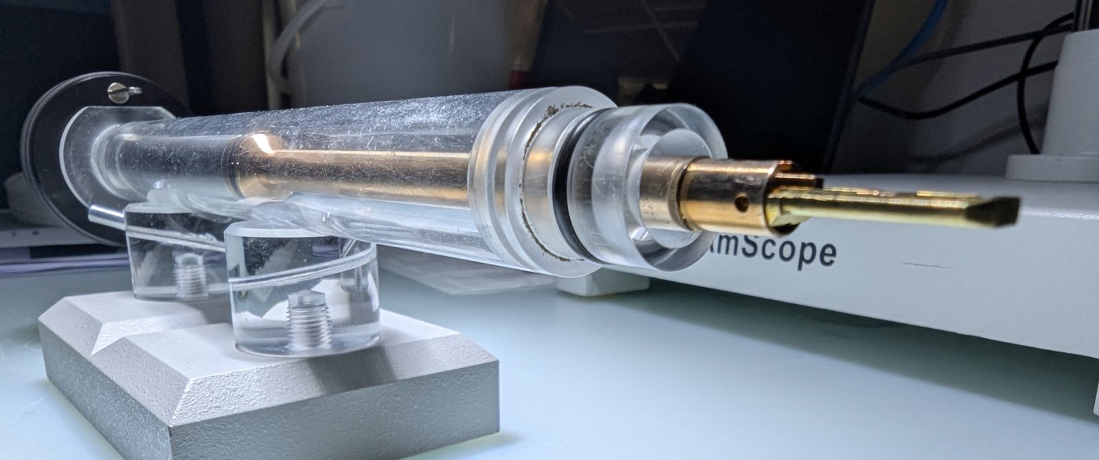
Key hardware components
-
Electron gun (source): Generates the primary electron beam used for scanning the sample.
-
Electromagnetic lenses: Focus and control the electron beam as it travels down the column toward the specimen.
-
Scanning coils: Deflect the focused electron beam in a raster pattern over the sample surface.
-
Specimen stage: Holds and allows precise positioning of the sample under the electron beam.
-
Detectors: Capture secondary electrons, backscattered electrons, or X-rays emitted from the sample to form images or analyze composition
-
Vacuum system: Maintains a high vacuum environment to prevent electron scattering by air molecules and ensure accurate imaging.
-
Control and imaging electronics: Manage beam parameters, data acquisition, and image display.
-
-
Sample preparation milestones
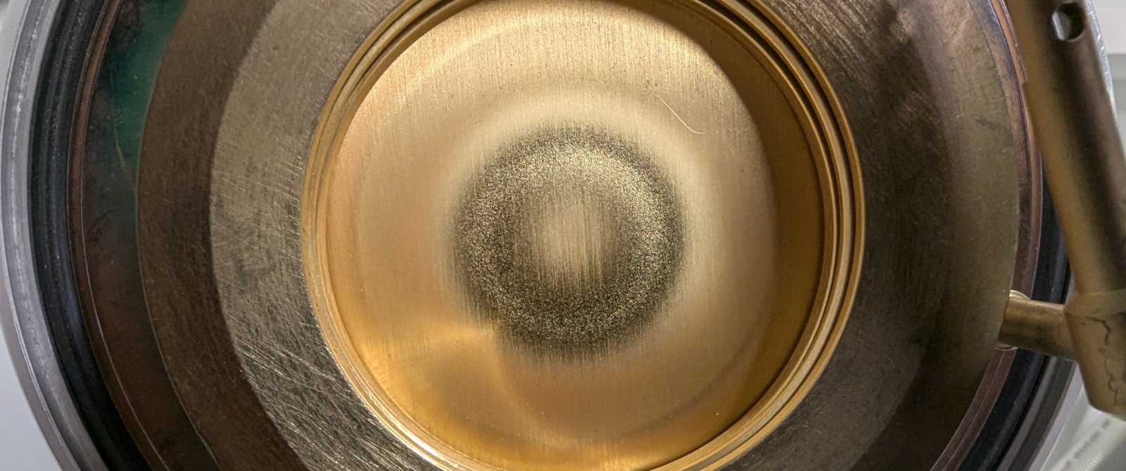
Conductivity
Gold sputter coating is a sample preparation technique for scanning electron microscopy (SEM) in which a very thin layer of gold (typically a few nanometers thick) is deposited onto the surface of a specimen to make it electrically conductive. This conductive coating helps to minimize charging effects and improve image quality when imaging non-conductive samples, as the gold layer allows electrons to dissipate rather than accumulate on the sample surface.
Water-free biological samples
If air-drying is not sufficient, several techniques for removing water from biological samples were developed.
Critical point drying
A critical point dryer for scanning electron microscopy (SEM) samples works by replacing the water in a biological specimen with a transitional fluid, usually liquid carbon dioxide, after dehydration. The sample is then brought to the critical point of the fluid—where liquid and gas phases are indistinguishable—allowing the fluid to be removed as a gas without passing through a liquid-gas interface. This process prevents surface tension forces that would otherwise cause delicate structures to collapse or distort during drying, thus preserving the specimen’s ultrastructure for high-resolution SEM imaging.

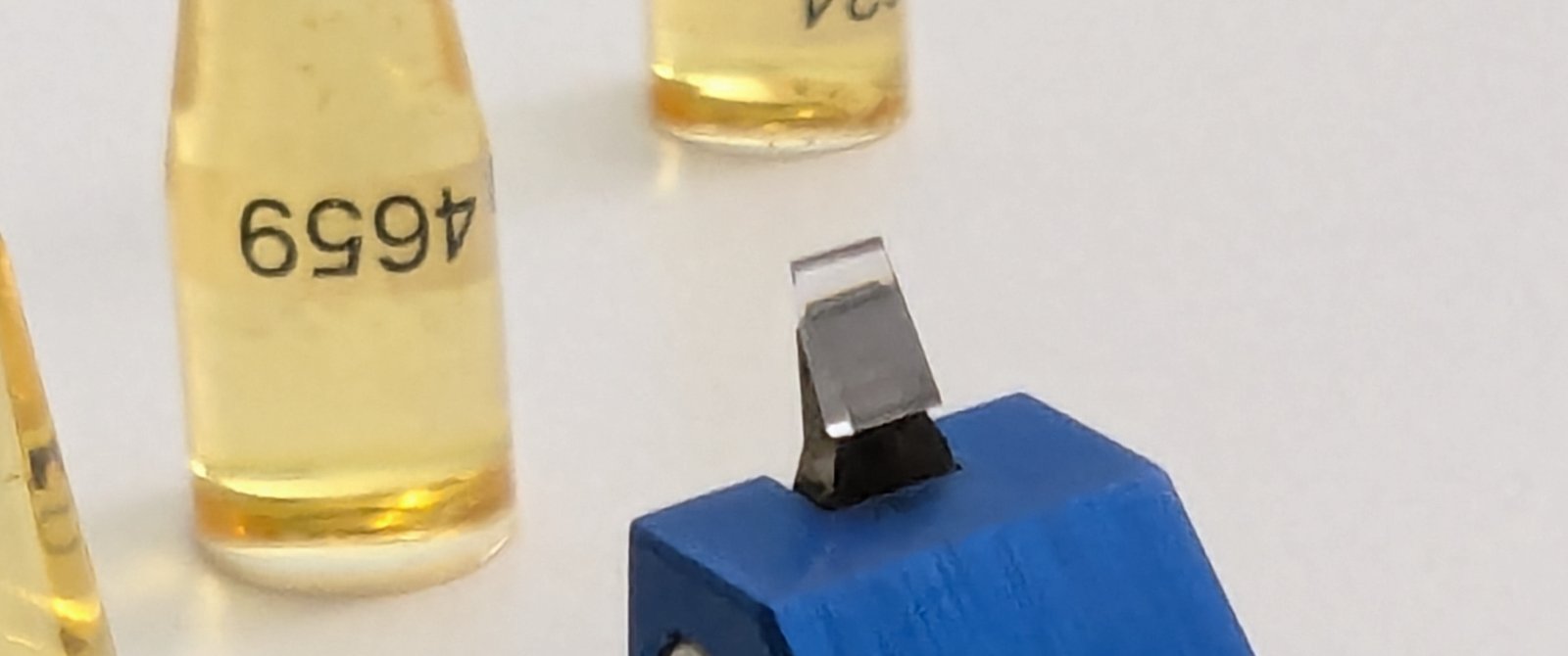
Click to enlarge Hexamethyldisilazane
Hexamethyldisilazane (HMDS) is a chemical often used as an alternative to critical point drying (CPD) for preparing biological samples for scanning electron microscopy (SEM). It allows for efficient drying of samples while preserving surface details, potentially reducing artifacts and making the process faster and less expensive than CPD.
HMDS has a low surface tension, which helps to minimize the collapse and distortion of tissues during drying, leading to better preservation of surface details. It is generally faster and does not require specialized equipment like CPD, which can be expensive. However, HMDS is flammable and volatile, so appropriate safety precautions should be taken when using it, such as using a fume hood and wearing protective equipment.
Focused ion beam scanning electron microscopy
-
Key hardware components
-
Focused Ion Beam (FIB) Column : Generates and focuses a beam of ions (commonly gallium) used for site-specific milling, cross-sectioning, and sample modification.
-
Scanning Electron Microscope (SEM) Column : Provides high-resolution imaging of the sample surface using an electron beam.
-
Sample Stage : Precisely positions and moves the sample for both imaging and ion milling operations.
-
Detectors : Capture secondary electrons, backscattered electrons, and ion-induced signals for image formation and analysis.
-
Vacuum System : Maintains the high vacuum required for both ion and electron beam operations.
-
Gas Injection System: Delivers precursor gases for processes like deposition or enhanced etching during FIB operations.
-
Control and Automation Electronics : Coordinate beam parameters, stage movement, data acquisition, and automated workflows, such as site-specific sample preparation
-
-
Sample preparation milestones
The sample preparation follows the same procinples asdetailed in SEM imaging above.
Transmission electron microscope
TEM provides unparalleled resolution for internal structures, making it indispensable for both nanomaterials and cellular ultrastructure studies.
-
Key Hardware Components
- Electron gun (source): Produces a beam of electrons that will be transmitted through the sample.
- Condenser lenses: Focus and control the electron beam before it reaches the specimen.
- Specimen holder and stage: Securely holds the ultra-thin sample and allows precise positioning and movement.
- Objective lens: Focuses the electrons that have passed through the specimen to form an initial image.
- Intermediate and projector lenses: Further magnify and project the image onto the viewing screen or camera.
- Imaging system (fluorescent screen, digital camera, or photographic film): Captures and displays the final image.
- Vacuum system: Maintains a high vacuum throughout the column to prevent electron scattering by air molecules.
- Control and alignment electronics: Manage beam parameters, lens currents, and image acquisition.
-
Sample preparation
Drop-casting
The dropcasting technique for preparing nanoparticles for transmission electron microscopy (TEM) involves depositing a small droplet of a nanoparticle suspension onto a TEM grid, usually coated with a thin carbon film. After allowing the droplet to air dry, the nanoparticles adhere to the grid surface, forming a thin layer suitable for electron transmission and imaging. This straightforward method enables rapid sample preparation for morphological and size analysis of nanoparticles, although care must be taken to avoid aggregation or uneven distribution during drying.
Epoxy embedding and ultramicrotomy
Ultramicrotomy is a sample preparation technique for transmission electron microscopy (TEM) in which an ultramicrotome—a precision instrument equipped with a diamond or glass knife—is used to cut ultra-thin sections (typically 50–100 nanometers thick) from a specimen embedded in a suitable resin (typically epoxys). These thin sections are required because electrons must be able to transmit through the sample for imaging in TEM.
Ultramicrotomy is widely used for biological samples such as cells and tissues, as well as soft materials like polymers, composites, and certain layered or coated materials. It can also be applied to some inorganic and composite materials, although very hard or brittle samples may present challenges and sometimes require alternative preparation methods. This technique is valued for producing large, uniform thin sections with minimal beam or chemical damage, making it ideal for high-resolution ultrastructural studies in especially life sciences.
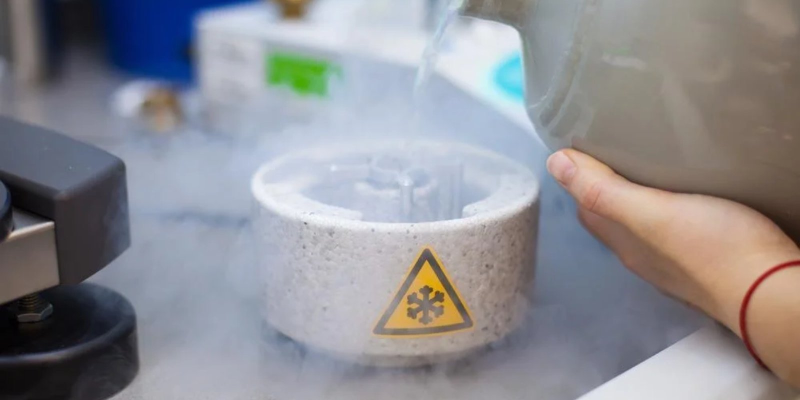
Cryoplunging (CryoTEM)
Cryoplunging is a sample preparation technique for transmission electron microscopy (TEM) in which a thin film of the sample, often a biological macromolecule, nanoparticle suspension or liposomal preparation, is rapidly plunged into a cryogen such as liquid ethane or propane cooled by liquid nitrogen. It is paramount that the medium is water and that the liquid is not viscous.
This ultra-rapid freezing process, known as vitrification, prevents the formation of ice crystals and preserves the sample in a close-to-native, hydrated state, making it ideal for high-resolution structural studies of proteins, viruses, organelles, and other sensitive biological or soft matter samples. Cryoplunging is especially valuable for studying structures that would be damaged or altered by chemical fixation or drying, and is a foundational step in cryo-electron microscopy (cryo-EM) workflows
The above-mentioned knowledge and technology led to the development and implementation of numerous microscopy techniques and different setups. In the table below, you will find a list of well-established microscopy techniques. Not all of these techniques are available through the core facility or a particular laboratory at our university. However, the microscopy core facilities in Switzerland are well networked. If a particular instrument is not available on campus, our staff will direct you to the closest core facility that has the instrument in question available.
| Technique | Microscopy platform | Sample | Reslution | Availability | Contact |
|---|---|---|---|---|---|
| Bright-field TEM | Transmitted electron microscopy | Thin (<100 nm), nanoparticles | 5Å | ||
| Dark-field TEM | Transmitted electron microscopy | Thin (<100 nm), nanoparticles, strongly scattering | 5Å | ||
| CryoTEM | Transmitted electron microscopy | Aqueous, cryoplunged samples | 5Å | ||
| Electron diffration / basic crystallography | Transmitted electron microscopy | crystalline sample | 75 pm | ||
| TEM tomography | Transmitted electron microscopy | mediusm thick sample (max about 250 nm) | 1 nm (in xy and z) | ||
| Analytical TEM | EDX1, EBSD2, EELS3 TEM | Thin (<100 nm),nanoparticles; | 5 nm | ||
| Secondary electron imaging | Scanning electron microscope | Bulk sample, conductive and water-free | 2-5 nm | ||
| backscattered electron imaging | Scanning electron microscope | Bulk sample, conductive and water-free | 2-5 nm | ||
| Electron dispersive X-ray spectroscopy | Scanning electron microscope | Bulk sample, conductive and water-free | 10-50 nm | ||
| Electron backscattered diffraction | Scanning electron microscope | Bulk sample, conductive and water-free | 300nm, 1μm |
||
| Cross section milling | Focused ion beam scanning electron microscope | Bulk sample, conductive and water-free | 2-5 nm, to max 30μm wide and 30μm deep | ||
| FIB Tomography / slice & view | Focused ion beam scanning electron microscope | Bulk sample, conductive and water-free | 2-5 nm in XY, 5-10 nm in z. Max 30μm x 30μm x 50μm | ||
| Lithography (e-beam and ion beam) | Focused ion beam scanning electron microscope | Relevant photoresist | 2 nm | ||
|
1: Energy dispersive X-ray spectroscopy 2: Electron backscattered diffraction 3: Electron energy loss spectroscopy |
: Available in core facilities : Existing in research labs : Not available on campus |
||||